
Precision thin film engineering

Thin Film Technology for Ceramic, Glass & Polymer Applications

Core metallization technology and precision processing for microwave, optical communication, power and advanced electronic applications.

About us

Experience built into every layer.

Thin film circuit substrate

Founded in 2010, OTF Technology Co., Ltd. develops and manufactures high-heat-dissipation, high-reliability thin film circuit substrates.

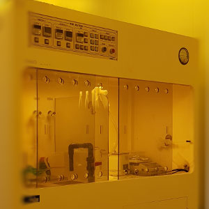
Our Suwon production environment includes Class 10,000 and Class 1,000 clean rooms. Engineers with more than 20 years of thin film circuit and MEMS process experience support stable, precise production.

2010Established
20+ yearsEngineering experience
ISO 9001Quality management
2010Company established
2013Thin film substrate supply
2015OLED test kit supply
2017Thin film production line established
201828 GHz BPF R&D selected
2019Single-layer capacitor supply

Products

Designed for demanding electronic applications.

From product design to mass production, OTF Technology Co., Ltd. supports development with precision processes and practical engineering.

01

Thin Film Product

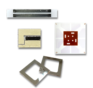
Microwave and RF application products manufactured on alumina, quartz, beryllia and sapphire substrates.
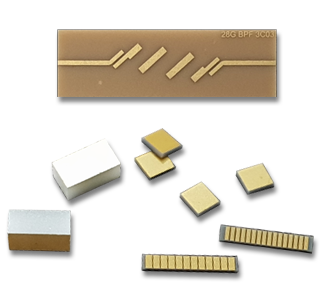
Thin film product collection
  1. Stand-off

    Wire-bonding pads, low-capacitance stand-offs and DC-bias connections for hybrid assembly.

  2. Thin Film Resistor

    Uniform NiCr and TaN resistors, laser trimmed for highly accurate resistance values.

  3. Single Layer Capacitor

    High-k single-layer and array capacitors for microwave circuits, DC blocking and RF bypass.

  4. Band Pass Filter

    Low-loss, precise thin-film filters developed for 5G and 28 GHz applications.

  5. 50-ohm Microstrip

    Low-loss transmission lines with stable performance across the 0–20 GHz range.
02

Custom Product

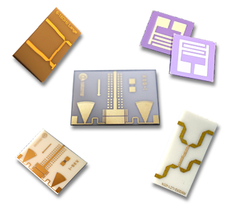
Application-specific thin-film circuits developed with precise and flexible processing technology.

Custom thin film circuits
  1. Combiner & Divider

    Compact microwave circuits designed around customer frequency and power requirements.

  2. Lange Coupler

    Fine-line coupled structures with controlled geometry and repeatable electrical performance.

  3. Custom Circuit

    Thin-film resistors, conductors and multilayer features integrated to customer drawings.

03

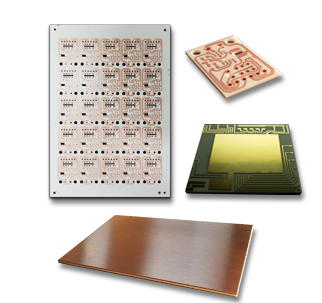
Ceramic PCB

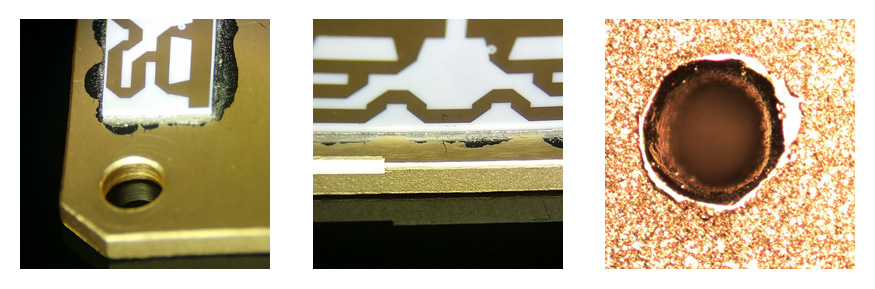
Durable ceramic circuit boards formed by printing, firing and precision PCB processing.

Ceramic PCB products
  1. LED & Lighting

    Thermally stable substrates for spotlights and high-current LED applications.

  2. Power Electronics

    High-insulation boards for converters, controllers and high-power transistor arrays.

  3. Automotive & Energy

    Reliable ceramic platforms for electric vehicles, motors and solar-cell applications.

04

Optics

Precision optical and display components produced with thin-film patterning technology.

Optics product collection
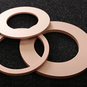
  1. Ceramic Submount

    Alumina or aluminum-nitride submounts, optionally supplied with Au-Sn eutectic solder.

  2. OLED Test Kit

    ITO-panel test kits for OLED process verification and material development.

  3. Optical Window

    Glass and quartz windows for photodiodes, laser diodes, LEDs and UV-C applications.

Services

One partner, from surface to finished component.

Thin film coating
01

Thin Film Coating

Metal, dielectric and multilayer coating using sputtering, evaporation and CVD processes.

Al · Cu · Au · Ag · Cr · NiCr · Ti · Pt · TaN
Photolithography
02

Photolithography

Photoresist coating and patterning for thin and thick PR, including dry-film processes.

Gold plating
03

Plating

Electroplating and electroless plating for wire bonding, die bonding and precision patterns.

Ceramic dicing
04

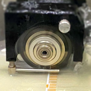
Precision Dicing

Controlled cutting for ceramic, glass and silicon substrates using application-specific blades.

Laser machining
05

Laser Processing

UV laser machining and resistor trimming for ceramics and thin film metal patterns.

Technology

A connected process, engineered for repeatability.

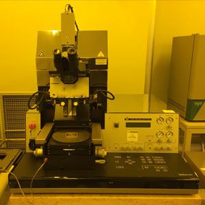
Cleaning, drying, deposition, photolithography, plating, etching, dicing and inspection are designed as one controlled flow. Process decisions are supported by experienced thin film engineers.

CleanDepositPatternPlateEtchDiceInspect
Thin film manufacturing process diagram

Contact

Bring us your next thin film challenge.

Tell us about the substrate, materials, dimensions and production requirements. Our team will review the application and respond by email.

info@otftechnology.com

OTF Technology Co., Ltd.

Suwon, Republic of Korea

For product, coating and precision-processing inquiries, contact our technical team by email.

Send an inquiry →